Memory Markets: Micron targets 42 Gb/mm2 with bonded wafers in 2027
The manufacturer expects to double storage density and increase input/output speeds by 50% in its next-generation flash memory.
By Carmen Wojcik ·
Micron Technology plans to begin mass production of its G11 3D NAND flash in the second half of 2027. The company announced the timeline at an industry event this week. The new chip will incorporate wafer-on-wafer bonding to achieve higher capacity and efficiency.
The G11 generation is designed to double the storage density of the current G9 product line. Micron projects the new technology will reach 42 Gb/mm2 in triple-level-cell form. This represents an increase from the current standard of approximately 21 Gb/mm2. Input/output speeds are expected to rise by up to 50%, moving from 3,600 MT/s to 5,400 MT/s. Energy consumption for data transfer should decrease by more than 25%.
The density improvements exceed the next-generation offerings from competitors Kioxia and Samsung. Kioxia is developing BiCS10, while Samsung is preparing V10. Micron states the G11 architecture will benefit high-capacity solid-state drives for client and data center applications. It will also support storage devices built for artificial intelligence workloads that require high bandwidth and low power usage.
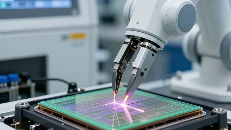
The primary technical shift involves bonding two separate wafers together. One wafer contains the NAND memory array, while the other holds the peripheral circuitry and input/output components. This allows Micron to use different manufacturing processes for each part. The company has used CMOS-under-array designs for several generations, but bonding provides greater freedom to optimize logic and memory independently.
Scott DeBoer, Micron's president and chief technology and products officer, confirmed the timing aligns with cost-effectiveness and product specifications. "This is the right timing for that technology," DeBoer said. He described G11 as the world's most advanced NAND. The design will include more than 400 layers, though the exact number of active wordlines has not been disclosed. Micron intends to provide further technical details in 2027 as high-volume production approaches.
Beyond the G11 launch, the company aims to scale in all three dimensions. Micron is developing high-mobility materials and ultra-dense cell architectures to improve transistor characteristics. DeBoer noted that the roadmap focuses on new materials and continued scaling of cell dimensions. He stated, "Beyond G11, we have a strong roadmap, not going to go into great detail on it today."
More Business · Tech news · Business Watchdog · Report a business · Got a Story?